Tuesday 30 September 2014

Arduino ATTiny84 ISP Shield – PCB – Part 1

Following on from my ATTiny84 ICSP Arduino Shield Plan article and in the same vein as the Arduino ATTiny85 ISP Shield articles, I am now in the process of making an Arduino shield for programming the ATTiny84. This is the 16 pin miniature Atmel microprocessor.

ATTiny84_Pinout_thumb1

The above shows the pin configuration of the ATTiny84 that the shield will interface to the Arduino. The relevant pins for ICSP control are Vcc, GND, PB3 (RESET), PA4 (USCK), PA5 (MOSI), and PA6 (MISO).

Once again, the design makes use of the Arduino Pins 7, 8 and 9 for PRG, ERR and HB indicator LED, so while the arrangement of pins is different, the function and interface to the Arduino UNO is the same.

Fritzing-ATTiny84-ICSP_etch_copper_b

The above image is the mirror reverse copper bottom layer converted to a jpeg file. And below is the toner transferred PCB that was created using the above (although, I’ve used the raster PDF version rather than the converted bitmap). Last night I discovered that I got this wrong. The copper trace on the bottom of the PCB should not be reversed. Make sure you print it out correctly. I still get this wrong from time to time.

ATTiny84-ISP-Shield-01_thumb1

I’ve since given the PCB a bit of a scrub with a wet thumb to remove the remaining paper residue and gone over the traces with a medium Staedtler Lumocolor marker to improve the resolution of the traces and pads.

Now all that remains is to etch the board and start populating it in the same manner as the ATTiny85 version.

I also made another 9V to 5V regulated power supply. The only difference that I am making to the new 5V reg is to orient the output +/- on the bottom of the PCB so that I can plug it directly into a solderless breadboard (meaning that I don’t have to chase wires from the reg to the board … more elegant, I think).

9V---5V-Regulator_thumb

Again, scrubbed with wet thumb and then retraced with the marker to give a better resist for the acid bath.

In case you are interested … here is the bitmap copper bottom mirror for transfer toner.

Fritzing-9V-to-5V-Regulator_etch_cop

Well … that’s it for me, tonight.

Dual Sided PCB – A first foray – Part 2

Eurgh … what a waste of effort.

I did the toner transfer onto the PCB that I cut into a circle and it was a disaster. I used a different printer and different paper and I think that the reason that the toner transfer didn’t work very well was a combination of those two factors.

Bottom Side

Top Side

This is what it looks like when the toner transfer doesn’t work properly.

I shouldn’t have rushed it, really … it’s my fault.

Back to the drawing board for this one. Fortunately, nothing is committed at this stage (except for the cutting of the PCB), so it isn’t a complete waste of material, just my time.

Oh well, you live and you learn.

Dual Sided PCB – A first foray – Part 1

Now that I am fairly confident in my ability to produce a single sided printed circuit board, it’s time to move on to the more complex issue of producing a 2 sided printed circuit board.

The plan is to make a circular PCB with a shift register and 8 LED. The circuit will be driven by an ATTiny85 that attaches via 3 jumpers to the board (so that I can free up some space on the board) and to power via another 2 jumpers.

Shift Register - Round PCB - Copper Both Layers

Above is the circuit design showing both the top and bottom layer.

I started out by using a hole saw to cut the double sided copper clad board to the right shape. The main downside to this method is that you end up with a pilot hole in the middle of the board. Fortunately, the pilot hole ends up underneath the 16 pin DIP and not much routing needs to be considered.

Normally, when transfer printing a single layer PCB, the bottom layer is printed out as a mirror image so that when it is transferred to the board, it’s around the right way. For dual layer, it seems that the top layer is printed out in positive and transferred to the PCB so that it will match up with the bottom layer. I printed out both top (positive) and bottom (mirror) onto an A4 sheet of paper, held the sheets with the toner side facing each other and held it up to the light and it looked like the above image … so I think that this is the right way to go.

I also included three “register” points on the design so that I could align the two faces. I plan to cut the A4 sheet down to the design and then hold both top and bottom layer to the copper clad board using the register points for aligning them.

The other three holes in the design are for mounting screws.

Shift Register - Round PCB - Copper Top

The top layer includes the ATTiny85 connections (4 o’clock on the design), most of the shift register connections and the anode connections for the LED.

Shift Register - Round PCB - Copper Bottom Mirror

The bottom layer includes the resistors (I’m using 0805 SMD), the cathode connections for the LED, and the power connections (note that the bottom layer as shown above is NOT mirrored … if you are going to use this design, you will need to mirror the image first).

One of the things that I haven’t quite worked out yet is the connection of the DIP on two layers. I may have to do some rearranging of traces, bending of DIP legs so that they can be surface mounted on the top layer.

This design requires:

  • 8 x 0805 SMD resistors (appropriate for your LED) I’m using 100Ω;
  • 8 x LED;
  • 1 x 16 pin DIP;
  • 1 x 3 pin header (connects to the ATTiny85);
  • 1 x 2 pin header (connects Vcc and GND);
  • 1 x 74HC595 Shift Register IC;

To run the circuit, I’m going to have the ATTiny85 on a solderless bread board running my modified Shift Register sketch.

Well … that’s the plan. I’ll do the toner transfer and etch tonight and see how far I get along with the build.

Saturday 27 September 2014

What is made most in the shed …

Today, I made some inroads into tidying up my shed/workshop.

The main task that I had to complete so that I could actually put my tools and materials in some kind of an order, was the creation of some shelving.

A couple of weeks ago the house next door was sold and the new owners told us that they intended to demolish and build a new house. BING! went my brain … material! I asked our new neighbours if I could salvage some floorboards before they carted it all to the tip. Our neighbours gave me a week to tear out whatever I wanted from the house before they demolished. Lucky, lucky me!

I didn’t get greedy, I went in with a purpose in mind. Floorboards = shelves.

Yesterday, I bought some batten pine and made up the frames for my shelves and it all went swimmingly. To make my shelves all even and level, I made one frame with 5 shelves and then clamped crosspieces to it and the legs so that every one of the four supporting pieces were the same. It also helped that I had two drills. One for drilling pilot holes, and another with a Phillips head drive in it to drive the screws into the holes.

Today I put it all together and I am pleased to say that my shelves are now firmly attached to the shed walls and sturdy. The shelves are only 2 floorboards wide, but that’s plenty wide enough for my tools. The shelves are about 3.5m long and 2.4m high with loads of space underneath the bottom shelf for my big metal toolboxes to fit (with the lid open … a design feature suggested by my darling wife).

Tonight, I started sorting out my stuff. I also put up a peg-board on one of the walls of the shed so that I can hang my hammers, saws and various often used tools.

Joy.

I reckon that the most commonly made thing in a shed/workshop is the humble shelf.

Wednesday 24 September 2014

Arduino – One Button Multiple Functions

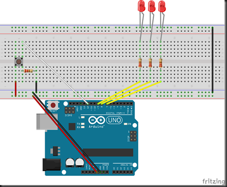
One of the things that I want to do with my LED functions is to control them with a single momentary switch. This means that I’ll have less hardware that the user needs to interact with, but the trade-off is that the user will need to press the button multiple times to get the function that they want.

The idea is to use a momentary switch that supplies current to the three LED functions (Glow, Chase, Lamp). I plan to do this by implementing an ATTiny85 to serve as a switch controller. First, though, the proof of concept is by controlling three LED with one momentary switch.

The breadboard is fairly straight forward. The Momentary Switch is connected to Pin 12 on the UNO and has a pull-down resistor. The three LED (acting as proxies for the ATTiny85 that will control the LED functions) connect to Pins 7, 8 and 9 on the UNO. When the button is pressed, a variable is incremented and passed to a switch statement, so that you get all possible combinations of the three LED (X00, 0X0, 00X, XX0, 0XX, X0X, XXX and 000) (I think).

One Button Three Functions

I’ve had a bit of a look around on the interweb and haven’t found anything startling … so I’ve used the basic Button example on the Arduino site and mixed it up with the switch control to arrive at a design that I think will work.

Most of the smarts for this happen in the sketch.

int buttonPin = 12;

int fi = 7;
int se = 8;
int th = 9;

int buttonPushCounter = 0;  
int buttonState = 0;        
int lastButtonState = 0;    

void setup()
{
  Serial.begin(9600);
  pinMode(buttonPin, INPUT);
  pinMode(fi, OUTPUT);
  pinMode(se, OUTPUT);
  pinMode(th, OUTPUT);
 
  digitalWrite(fi, HIGH);
  digitalWrite(se, HIGH);
  digitalWrite(th, HIGH);
  delay(300);
  digitalWrite(fi, LOW);
  digitalWrite(se, LOW);
  digitalWrite(th, LOW);
}

void loop()
{
// read the pushbutton input pin:
  buttonState = digitalRead(buttonPin);

  // compare the buttonState to its previous state
  if (buttonState != lastButtonState) {
    // if the state has changed, increment the counter
    if (buttonState == HIGH) {
      // if the current state is HIGH then the button
      // wend from off to on:
      buttonPushCounter++;
      if(buttonPushCounter == 9){ buttonPushCounter = 1;}
      Serial.println("on");
      Serial.print("number of button pushes:  ");
      Serial.println(buttonPushCounter);
    }
    else {
      // if the current state is LOW then the button
      // went from on to off:
      Serial.println("off");
    }
  }
  // save the current state as the last state,
  //for next time through the loop
  lastButtonState = buttonState;
  switch(buttonPushCounter)
  {
    case 1:
      digitalWrite(fi, HIGH);
      digitalWrite(se, LOW);
      digitalWrite(th, LOW);
      break;
    case 2:
      digitalWrite(fi, LOW);
      digitalWrite(se, HIGH);
      digitalWrite(th, LOW);
      break;
    case 3:
      digitalWrite(fi, LOW);
      digitalWrite(se, LOW);
      digitalWrite(th, HIGH);
      break;
    case 4:
      digitalWrite(fi, HIGH);
      digitalWrite(se, HIGH);
      digitalWrite(th, LOW);
      break;
    case 5:
      digitalWrite(fi, HIGH);
      digitalWrite(se, LOW);
      digitalWrite(th, HIGH);
      break;
    case 6:
      digitalWrite(fi, LOW);
      digitalWrite(se, HIGH);
      digitalWrite(th, HIGH);
      break;
    case 7:
      digitalWrite(fi, HIGH);
      digitalWrite(se, HIGH);
      digitalWrite(th, HIGH);
      break;
    case 8:
      digitalWrite(fi, LOW);
      digitalWrite(se, LOW);
      digitalWrite(th, LOW);
      break;
  }
  Serial.println(buttonState);
}

I think that I can probably simplify the code a bit more, but it works OK. The only real problem that I have with this code is that the button press has to be fairly confident … a little press does nothing.

I guess that you could scale the number of functions up to the number of pins that you have available, or maybe a shift register? Dunno, I haven’t tried that yet.

The next step with this design is to replace the 3 LED with 3 ATTiny85 to see if that works. The plan is to connect Vcc on the ATTiny85 to Pins 7, 8, 9 of the UNO, if it works the way I hope, then the button press will turn each of the ATTiny85 on and off according to the switch statement. We’ll see.

Saturday 20 September 2014

ATTiny85 – Chasing LED sketch – Revised

I wanted to make the chasing LED sketch more efficient so that I could reuse the code for chained Shift Register (74HC595) chips without having to touch the code much.

There is really only one change that needs to be made programmatically to do this (I think). I figured that, if I set the number of LED in a variable in the header of the sketch, that this would be the only place that needs to be updated.

Of course, to prove this, I’m going to need to get another 74HC595 chip and connect it up (with the additional LED and resistors. So, at the moment, this is really only theoretical.

In addition to setting the number of LED in a variable, I’ve changed the “for” loop to a “while” loop, that’s really just preference, but you’ll see what it does in the code.

/*
  Shift Register Chasing LED
  Sends the data value to the shift register to
turn each
  LED on in turn for a chasing lights circuit
*/
int latchPin = 2;  // connected to ST_CP (12) of 74HC595
int clockPin = 3;  // connected to SH_CP (11) of 74HC595
int dataPin = 0;   // connected to DS (14) of 74HC595

int nLED = 8;      // 8 LED connected to the array
int nPause = 60;   // the delay between each cycle

byte data;

void setup()
{
  pinMode(latchPin, OUTPUT);
  blinkAll_2Bytes(2, 500);
}

void loop()
{
  int i = 0;
  byte ledValue = 1;
  while( i < (nLED))
  {
    digitalWrite(latchPin, 0);
    shiftOut(dataPin, clockPin, ledValue);
    digitalWrite(latchPin, 1);
    delay(nPause);
    ledValue = ledValue * 2;
    i++;
  }
}

void shiftOut(int myDataPin, int myClockPin, byte myDataOut)
{
  int i = 0;
  int pinState;
  pinMode(myClockPin, OUTPUT);
  pinMode(myDataPin, OUTPUT);
  digitalWrite(myDataPin, 0);
  digitalWrite(myClockPin, 0);
 
  for(i = nLED-1; i>=0; i--)
  {
    digitalWrite(myClockPin, 0);
    if (myDataOut & (1<<i))
    {
      pinState = 1;
    }
    else
    {
      pinState = 0;
    }
    digitalWrite(myDataPin, pinState);
    digitalWrite(myClockPin, 1);
    digitalWrite(myDataPin, 0);
  }
  digitalWrite(myClockPin, 0);
}

void blinkAll_2Bytes(int n, int d) {
  digitalWrite(latchPin, 0);
  shiftOut(dataPin, clockPin, 0);
  shiftOut(dataPin, clockPin, 0);
  digitalWrite(latchPin, 1);
  delay(200);
  for (int x = 0; x < n; x++) {
    digitalWrite(latchPin, 0);
    shiftOut(dataPin, clockPin, 255);
    shiftOut(dataPin, clockPin, 255);
    digitalWrite(latchPin, 1);
    delay(d);
    digitalWrite(latchPin, 0);
    shiftOut(dataPin, clockPin, 0);
    shiftOut(dataPin, clockPin, 0);
    digitalWrite(latchPin, 1);
    delay(d);
  }
}

The “while” loop starts with a ledValue of 1 and, for each loop, it multiplies ledValue by 2 to get the next lamp ID (1, 2, 4, 8, 16, 32, 64, 128) and it increments “i” stopping when i = nLED. The ledValue is a byte value and this is sent to the shiftOut function.

Secondly, the “for” loop in the shiftOut function also takes the number of LED (nLED) as a control value to set the pin state.

The other change that I’ve made to the sketch is to set the delay value as a variable in the sketch header so that I can change that value quickly, without having to hunt for it in the code.

Anyway, I’ll come back to this sketch when I’ve put in the second shift register (not until next week, I’m afraid … I’m off on holidays right now and several hundred kilometres away from my equipment and components).

Friday 19 September 2014

ATTiny85 Tutorial 3 – Reading Digital (On/Off) Input

I’m still trying to find the time to do these tutorial projects in amongst the rest of the things that I’m doing … so here goes with Tutorial 3 – Reading Digital (On/Off) Input for the ATTiny85.

The main thing to note here is that I’m only using 4 LED rather than the 8 LED that you will find in the Freetronics tutorials. Of course, that’s because the ATTiny85 doesn’t have the masses of pins that the UNO does, so I’ve scaled it back to 4 LED and modified the sketch accordingly.

The other thing to consider is that the available pins for the ATTiny85 are enumerated differently, so, rather than having pins 6 through to 13, we have pins 0 – 4. I need to use one of those pins as a digital input, so that leaves me with 0 – 3.

ATTiny85 Pin assignment

I’ve marked out the pins with the associated sketch variable so that you can see at a glance what connects where.

And here’s the sketch that I loaded onto the ATTiny85 (using my handy-dandy ATTiny85 ICSP from my previous article).

int ledCount = 4;
int ledPins[] = {0,1,2,3};
int ledDelay = 300;
int buttonPin = 4;

void setup() {
  for(int thisLed = 0; thisLed < ledCount; thisLed++) {
    pinMode(ledPins[thisLed], OUTPUT);
  }
  pinMode(buttonPin, INPUT);
}

void loop() {
  for(int thisLed = 0; thisLed < ledCount; thisLed++) {
    digitalWrite(ledPins[thisLed], HIGH);
    delay(ledDelay);
    while(digitalRead(buttonPin) == HIGH) {
      delay(10);
    }
    digitalWrite(ledPins[thisLed], LOW);
  }
}

The sketch initialises the ledCount variable, the ledPins integer array, the ledDelay and the buttonPin variable. The setup function sets the led pins as output and the button pin as input.

The loop cycles through the array making each LED turn on and then turn off, when the LED is HIGH, if the momentary button is held down, the LED stays HIGH until the momentary button is released, then it just keeps going through the cycle.

Project3

As you can see from the above image, the wiring for this circuit is also pretty straight forward. You will note in the top right hand corner, I’m using my 9V to 5V power regulator mini-board. This is another circuit that I completed in a previous post.

This is a very simple tutorial and it does not require any hard to find parts. Instead of using my regulator, I could have connected the positive rail to the 5V of the Arduino and the negative rail to the GND of the Arduino and then slaved the power from the Arduino via a USB connection to my computer, that’s OK and it’s the easiest way to do it if you don’t already have a 5V regulated power supply. Also, you could have breadboarded the ICSP rather than using a dedicated circuit … but since I have them and I built them for this purpose … I’m going to use them!

Well … there you go, Tutorial #3 – Reading Digital (On/Off) Input converted for the ATTiny85 for your entertainment and my fun.

Check out the rest of the tutorials here.

ATTiny85 ISP For Transfer Printing

Here are the toner transfer images for the Arduino to ATTiny85 ISP.

These images are unscaled so, when you print them, make sure that you print them without scaling (make sure your printer isn’t going to make the image “fit” the page.

The mirrored copper bottom of the board.

Fritzing ATTiny85 ICSP_etch_copper_bottom_mirror

and the silk top of the board.

Fritzing ATTiny85 ICSP_etch_silk_top

I’ve printed from the PDF output from Fritzing, so I cannot guarantee that these will work properly. I would recommend that you print the copper bottom out and then see if it matches up with the pin outs of the Arduino (or clone) that you are using.

These images relate to the Arduino ATTiny85 ISP Shield PCB article.

Tuesday 16 September 2014

ATTiny85 Tutorial 2 – Controlling 5 LED

This tutorial expands on the simple blinking LED by adding more LED to the board. One of the challenges with using the ATTiny85 is that there are far fewer pins that you can use to do stuff. This is, of course, also an advantage as it means that the ATTiny85 is much smaller and, therefore, more practical in small spaces. You have a greatly reduced footprint to shove into small appliances.

To keep to the spirit of the Freetronics tutorial, I have reduced the number of LED from 8 to 5, as that is the maximum number of pins that can be used without reassigning the RESET (PCINT5) pin. The RESET pin is able to be reassigned, however, changing it back to RESET requires high voltage programming and I’m not going into that here.

So, the connections and layout part.

Lesson 02 - Controlling 5 LED_bb

The pin scheme is fairly straight forward

  • LED 1 connects to PIN 5
  • LED 2 connects to PIN 6
  • LED 3 connects to PIN 7
  • LED 4 connects to PIN 2
  • LED 5 connects to PIN 3

The cathode of each LED connects to a resistor, each resistor connects to the ground rail.

The sketch is also quite straight forward. Instead of assigning the pin ID to a static variable, we are assigning it to an array and then iterating through the array step by step turning the LED HIGH and then, after the defined delay, back to LOW.

/*
  Control 5 LED
*/
int ledCount = 5;
int ledPins[] = {0, 1, 2, 3, 4};
int ledDelay = 125;

// the setup routine runs once when you press reset:
void setup() {               
for (int thisLed = 0; thisLed < ledCount; thisLed++)
  {
    pinMode(ledPins[thisLed], OUTPUT);    
  }
}

void loop() {
  for (int thisLed = 0; thisLed < ledCount; thisLed++)
  {
    digitalWrite(ledPins[thisLed], HIGH);
    delay(ledDelay);
    digitalWrite(ledPins[thisLed], LOW);
  }
  for (int thisLed = ledCount; thisLed > 0; thisLed--)
  {
    digitalWrite(ledPins[thisLed], HIGH);
    delay(ledDelay);
    digitalWrite(ledPins[thisLed], LOW);
  }
}

There were some errors in the Freetronics sketch that meant that copy and pasting was not practical. There was a trailing “\” character and the loop variable for the ledCount contained a typo. The above code works and has been tested … feel free to copy/paste it if you want … or just type it out, it isn’t long.

The code will result in each LED illuminating in turn for 125 milliseconds in a kind of scanning LED fashion.

Check out the rest of the tutorials here.

Monday 15 September 2014

ATTiny85 Tutorial 1 – Control an LED

The first tutorial that pretty much everyone covers is the “Hello World” tutorial of physical programming … connecting a single LED to the microprocessor and causing it to blink.

This is a very simple project and the outlook is sunny.

For this tutorial, you will need to prepare your ATTiny85 with the Blink sketch that comes with the Arduino IDE. This sketch uses the Arduino Pin 13 as the output pin, however, the ATTiny85 doesn’t have a Pin 13. To hook up our ATTiny85, we’re going to need to work out which pin would be compatible with the Arduino Pin 13. So … what are the characteristics of Arduino Pin 13? Pin 13 kinda special, apart from being a Digital interface, it is also an SPI pin (MOSI – Master Out Slave In) for asynchronous communication … typically used for data connection, like when you are connecting your ATTiny85 to the ATMegaxxxx for programming. For this tutorial, you don’t need to access that functionality, but we are looking for a Digital pin on the ATTiny85

ATTiny85_Pinout

The above shows the pinout scheme for the ATTinyx5. We could use PCINT0, PCINT1, PCINT3, PCINT4 or PCINT5 (or … any pin that isn’t VCC or GND). For simplicity sake, we’ll use PCINT0.

Having decided on which pin we are going to use as output in our experiment the next step is to change the example sketch.

Open the example sketch File > Examples > 01. Basics > Blink in the Arduino IDE

IDE_LoadBlink

The sketch that is loaded is the basic blink sketch

The only change that needs to be made to the example sketch is the pin variable

So you change:

int led = 13;

to

int led = 0;

And then you can upload the sketch to the ATTiny85 (remembering to first set up the Arduino as an ISP as per the previous article (Arduino as ISP for ATTiny85).

When the sketch is loaded, you can pop the chip out of the ISP shield and put it in your breadboard as per the following diagram.

Lesson 1 - Controlling an LED_bb

By convention, I’m using the Fritzing example 5V regulator (with the added 9V battery) to show the input source. Practically, I use my 5V regulator board from my previous article in it’s place.

The ATTiny85 is oriented with the dot bottom left, make sure that you orient your chip and connections correctly.

A jumper wire connects PCINT0 to the LED anode and the LED cathode is connected to the GND rail via a resistor (I’m using a 220 ohm resistor, but you should use the correct resistor for your LED).

When the power is connected, the LED blinks.

That concludes the first tutorial. I recommend that you also read the Freetronics tutorial so that you can compare the ATTiny85 implementation with the UNO clone implementation.

Check out the rest of the tutorials here.

Sunday 14 September 2014

Freetronics Eleven Tutorial to ATTiny85

Right-o … now that I have my Arduino to ATTiny85 ICSP working, it’s time to start working out the practical differences between the Arduino and the ATTiny85.

When I bought my Freetronics Experimenters Kit from Jaycar, the kit came with an Experimenters Guide (Experimenters Kit - Getting Started Guide). The guide, whilst basic, was very helpful and was quite good. The guide is designed to give the experimenter some confidence in the platform and their own ability, so … job done.

What I plan to do is to work through the 11 tutorials in the guide and apply them to the ATTiny85. Some tutorials have to be modified right from the get-go because of the simple fact that there aren’t as many pins on the ATTiny85 as there is on a UNO or UNO clone board. The one that I’m thinking of here is “Project 2: Controlling 8 LEDs”. Sure, you can control 8 LED with an ATTiny85, but the tutorial is about handling each LED from a single pin. This could be done using a shift register or charlieplexing, but that isn’t in the spirit of the tutorial, so instead this will be “Controlling 6 LED”.

I won’t be going over the ICSP and uploading sketches to the ATTiny85, that was pretty much covered in the Arduino ATTiny85 ISP articles.

I will preface each of the tutorials with the pertinent information from the original tutorial and show the converted breadboard layout and sketch from the perspective of the programmed ATTiny85.

Because of the absence of the UNO in the tutorial, it is expected that the breadboard will take it’s power source from a 5V regulated power supply. I recommend that, if you want to build these tutorials, that you also build that circuit (9V to 5V voltage regulator).

Basic with 5V Reg_bb

The first Tutorial “01 - Controlling an LED” is the simple blink sketch and really doesn’t need much explanation, however, I will be starting with this tutorial as a basic building block tutorial and it may prove useful to some.

I am also considering doing the same thing with an ATTiny84 so that there will be a source of these tutorials on the Interweb where people who are interested in starting out with the 84 and 85 can come and see the tutorials from the perspective of the platform that they are using.

Anyway … on with the show.

Saturday 13 September 2014

Arduino ATTiny85 ISP Shield – PCB – Part 3

Alrighty, following on from my previous post (Arduino ATTiny85 ISP Shield - Part 2), I’ve discovered that the trace on my board for PB1 to Pin 11 was faulty (the toner transfer wasn’t all that good). This resulted in the Arduino reporting an incompatibility error when using the Arduino ISP sketch to upload a sketch to the ATTiny85.

The solution was to “draw” solder along the trace to fix the continuity.

To do that, the copper is heated with the soldering iron and the flux makes the solder to stick to the trace. I call it “drawing” because you are kinda drawing solder on with the iron. Where the copper has pitted too much, the flux doesn’t bond to the copper very well, so I had to go over the trace a couple of times to get a reasonably thick solder line.

I went over the trace a couple of times and built up a continuous line of copper across the break in the line and tested the continuity a couple of times until I got a good signal from the pin to the socket.

The next thing that I did was that I went over the entire board and patched bit’s that looked a little dodgy and where the solder fillets were not quite good enough.

Finally, I plugged in an ATTiny85 chip, connected the shield to the UNO (this time I used the Freetronics Eleven clone), connected the UNO to my PC and launched the Arduino IDE.

First, I loaded the Arduino ISP sketch to the UNO and then I changed the board to ATTiny85 (1MHz clock) and the programmer to the Arduino ISP setting and uploaded the blink sketch to the ATTiny85.

The LED all lit up at the correct time and the IDE reported the usual avrdude miss-error … I am now a happy camper. The design worked, the production of the board worked and finally, the upload of the sketch to the ATTiny85 worked too … woo-frickin-hoo!

Thursday 11 September 2014

9V to 5V Voltage Regulator – PCB

In my previous article (9V to 5V Voltage Regulator Plan) I was working on making a small, discrete 5V power regulator with a 9V input voltage. Today, as I had some etchant going to waste, I decided to make this handy little circuit.

I started with toner transfer and then etched the board. After cleaning off the toner and drilling the through-holes, I printed out the silk and glued it to the top of the PCB and set to populating it.

The circuit uses:

  • 1 x LM705;
  • 2 x 100nF electrolytic capacitors;
  • 4 x pin headers
  • 1 x 18mm x 20mm FR4 single sided copper clad board

The soldering was very easy on this board, while it is a little cramped, I started with the pin headers, then the capacitors and finally the regulator.

9V_5V_VoltageRegulator_01

The input is at the back of the circuit and the output is at the front. I’ve labelled the +/- of the input/output as well as the expected voltage.

The datasheet for the LM7805 says that the input voltage range is 5V to 18V, but the goal for this little circuit is to be embedded in other devices that will have a 9V battery … so I’ve labelled it 9V. If you wanted to use this circuit with other voltages, please be sure that you read and follow the data sheet for the LM7805 (from www.fairchildsemi.com).

As I don’t have my multimeter with me, the only real test that I can perform is a voltage output presence test … that is, if I plug in a battery at input and a load at output, does the load circuit work.

As is fairly usual with my testing, I use my 2 x 2 SMD LED circuit as the load. I plugged in the battery and the load circuit and … light!

9V_5V_VoltageRegulator_02

I will do some actual voltage tests on the circuit next week when I am in the same state as my multimeter. For now, that’s job done.

This circuit will normally be wired up to feed power to a solderless breadboard when I need a regulated 5V supply, such as when I am testing my ATTiny84/ATTiny85 circuits. I’ll probably make a 3.3V version at some stage, but for now I don’t need one.

Here it is connected to the previously programmed ATTiny85 again, feeding the 2 x 2 SMD LED circuit.

9V_5V_VoltageRegulator_03

I’ve videoed the LED. This is using a modified version of the pulse function found in the ArduinoISP sketch. The pulse function drives the Heartbeat LED in the source sketch.

9V Battery 5V Regulator – ATTiny85 Power Supply

Oh, and by the way, here is the pulse sketch from the ArduinoISP sketch. The values following the comment (//) are the original values from the Arduino sketch, for reference.

int LED_HB = 0;

//void pulse(int pin, int times);

void setup() {
  pinMode(LED_HB, OUTPUT);
  pulse(LED_HB, 2);
}

uint8_t hbval = 175; //128;
int8_t hbdelta = 16; //16;

void heartbeat() {
  if (hbval > 225) hbdelta = -hbdelta; //192;
  if (hbval < 16) hbdelta = -hbdelta; //16;
  hbval += hbdelta;
  analogWrite(LED_HB, hbval);
  delay(50); //30;
}

void loop(void){
  heartbeat();
}

#define PTIME 50
void pulse(int pin, int times) {
  do {
    digitalWrite(pin, HIGH);
    delay(PTIME);
    digitalWrite(pin, LOW);
    delay(PTIME);
  }
  while (times--);
}

Arduino ATTiny85 ISP Shield – PCB – Part 2

Okay, I’ve now got some etchant, yay!

I tried to use the old etchant, but it was not working well at all. I went and bought some peroxide and some hydrochloric acid. The acid is from the same company that I usually buy, but now it seems they’ve added some iron salts to it (it’s a brick cleaner) and that results in the acid turning red when it mixes with the hydrogen peroxide. It still etches well enough, so, no harm. Interestingly, the hardware store no longer sells the 500ml bottles, their smallest bottle is 2.5L.

Anyway, I etched the board (and another so that I wasn’t wasting the etchant) and it turned out pretty well. I’ve also learned that agitating the acid bath makes it work better (faster) and the etch took just under 10 minutes.

ATTiny85_ISP_ShieldCopper_01

I then went ahead and did a transfer of the silk side.

ATTiny85_ISP_ShieldSilk_01

Which looked like crap.

So I came up with the idea to simply print the silk out and glue it to the top face of the PCB. I painted on a watered down solution of PVA first and then laid the paper on the board, next, I painted the PVA over the top of the paper too, so that it would wear better.

ATTiny85_ISP_ShieldSilk_02

Now I can actually read the silk side better. Nice. I don’t know that it will stand soldering very well though.

ATTiny85_ISP_ShieldPinsBeforeSolder

The pins were put into the board and the plastic blocks were slid up the headers to allow space for soldering.

ATTiny85_ISP_ShieldPinsAfterSolder

After soldering, the plastic blocks were returned to their previous position.

ATTiny85_ISP_Shield_R3Fit

I then tested that the pin headers matched up correctly with the Freetronics Eleven r3 (Arduino clone). They fit nicely, so it’s on to populating the board.

ATTiny85_ISP_Shield_Populated

I started with the resistors, then the 8 pin DIL and finally the LED. There was a bit of a problem with the LED, but it doesn’t stop the board working as an ISP. Actually, two problems. 1) the copper came away from the board, and 2) I got the LED backwards (face palm).

ATTiny85_ISP_Shield_UnoFit

Next, I plugged the shield into the Arduino UNO R3 (genuine) and it fitted well too.

I plugged it all in, loaded the Arduino ISP sketch onto the UNO and then tried to load the blink sketch onto the ATTiny85. No success. My multimeter is in another state at the moment, so I can’t figure out where the problem is. Oh, well … I’ll wait until next week to test the board properly and find out where I went wrong.

Well … I’ve made another PCB for this circuit (with the LED around the right way) and I no longer get the sync error, so that does make a difference. I’m getting an invalid signature error on the new board so it looks like there may be a continuity error somewhere. That’ll definitely have to wait until I’m with my multimeter again.

Now that I’ve done a continuity test of the circuit with the multimeter, I’ve found that the MOSI connection (Arduino Pin 11 to ATTiny85 PB1) is broken. I’m going to need to either solder over the break or get a conductive pen to fix it. Jaycar has a silver conductive pen for $30 … it seems a bit expensive. I think that I’ll go with solder.

Wednesday 10 September 2014

Arduino ATTiny85 ISP Shield – PCB – Part 1

As promised in Arduino as ISP for ATTiny85 – PCB Revisited, I have transfer printed the design onto a FR4 single sided copper clad board using the modified design.

ATTiny85_ISP_ShieldPCB_01

There were some missing bits in the transfer (as happens from time to time), so I went over the entire trace with a fine Staedtler Lumocolor permanent marker. The Lumocolor is really only ever a backup to toner transfer printing, but I have had some pretty good results using both of them before (Resistance is Not Futile!). You can also see that I’ve filled in the soldering points, that’s so that when I solder, the fillets are stronger (in my humble opinion).The above photo is not too bad, I’ve used a bright white overhead light to illuminate the subject, otherwise it looks like this …

ATTiny85_ISP_ShieldPCB_02

Anyway, enough talk of photography. I didn’t get around to buying any etchant … too poor at the moment, so it’ll have to wait. However, I decided to use some “old” etchant that I haven’t thrown away yet. It should still work, it will probably just take longer and need more agitation than a fresh batch. I guess I’ll find out.

I’ve also printed out the silk layer for applying to the other side. The trick with this is that the copper layer is printed as a normal image, whereas the silk layer is printed as a mirror image. That way, when the two are transferred, they are oriented correctly.

When (if) the etch is finished, I’ll clean the PCB down (acetone and then isopropyl alcohol) and transfer print the silk layer on the top of the PCB and add the pictures of the progress to this article.

Now it’s back to watching telly while I wait for the etch to bite.

Arduino as ISP for ATTiny85 – PCB Revisited

I have revisited the PCB design for the ATTiny85 ISP shield after trying it out a couple of times.

My design goal was to create a shield module for my Arduino R3 that I can use to program an ATTiny85 and that makes use of the indicator LED that are included in the ArduinoISP sketch (that comes with the Arduino IDE).

The bill of materials is fairly small and should be fairly inexpensive.

  • 1 x 8 Pin DIL socket ($0.17)
  • 1 x ATTiny 85 chip ($2.00)
  • 3 x 3mm LED (green, red, blue) ($0.12)
  • 3 x pin headers (2, 4 and 6 pin) ($0.12)
  • 3 x 220 Ω resistors ($0.03)
  • 1 x  40 x 53.5 mm copper clad F4 board ($0.17)

For a total of $2.61 (based on the cost of purchasing these items from eBay).

I plan to use this over and over again, so the cost of the ATTiny85 isn’t really part of the bill of materials, but I’ve included it for completeness sake.

Fritzing ATTiny85 ICSP_pcb

Also, there are some header pins that are only included to give the board a bit more mechanical structure (Arduino connections to pin 6, 3.3V and a GND connection). If you wanted to, you could save yourself $0.03 and not include them, but the shield would be wobbly.

While designing the PCB, I had the Arduino R3 part on in the design so that I could align the header pins correctly. I’ve printed the design out so that I can confirm the alignment. Also, if you really wanted to, you could remove the 3 x LED and associated 220 Ω resistors, but again, why not use them?

The PCB is single sided, so all of the traces should end up on the bottom of the board. The thing that I’ve been struggling with is that the header pins are soldered into the bottom of the board. This makes it a bit challenging to solder as the plastic block for the header pins will make contact with the copper side of the board, making it more difficult to solder. I will push the pins further into the plastic block and put the block on the component side of the PCB. However, that means that the solder fillet will interfere with the insertion of the pins into the Arduino. All that that really means is that the board won’t sit flush against the Arduino … meh.

I’ve put big friendly text on the PCB so that it is all pretty lookin’ when I’m done.

The solderless breadboard edition of the ATTiny 85 / ArduinoISP works pretty well, so I’ll be starting this project tonight. The only thing holding me up at this stage is that I’m out of Hydrogen Peroxide and Hydrochloric Acid at the moment, and I have to go to the Chemist and the Hardware store to restock (bummer). Well, the plan for tonight is to do the transfer printing of the PCB copper side. I won’t do the component side as it will just smudge when I use acetone to clean off the toner from the copper side.

Paypal Donations

Donations to help me to keep up the lunacy are greatly appreciated, but NOT mandatory.